
Complex PCB Design & Layout for your next successful product
Independent board designer specializing in FPGA, MCU, communication and mixed-signal boards. Production-ready layouts with controlled impedance, signal integrity and DFM built in from the first pass.

SERVICES
DESIGN & LAYOUT
Schematic capture through routed layout — placement, stack-up, signal integrity, and DFM checks built in from the first pass.
REVIEW
A second, experienced set of eyes on someone else's schematic or layout — errors, footprint mismatches, and risky nets flagged before fab or reverse engineering.
SIMULATE
Circuit-level and power simulations to confirm a design behaves as intended before a single board gets ordered.
CAPABILITIES
TECHNICAL SPECS
- Multi-Layer PCBs
- Rigid-Flex PCBs
- High-Density Placement
- Signal Integrity
SOFTWARE
- Various CAD Software
PROCESS
- Design and BOM creation
- Simulation and verifying design
- Stack-up and mechanical considerations
- Export and preparing to manufacturing
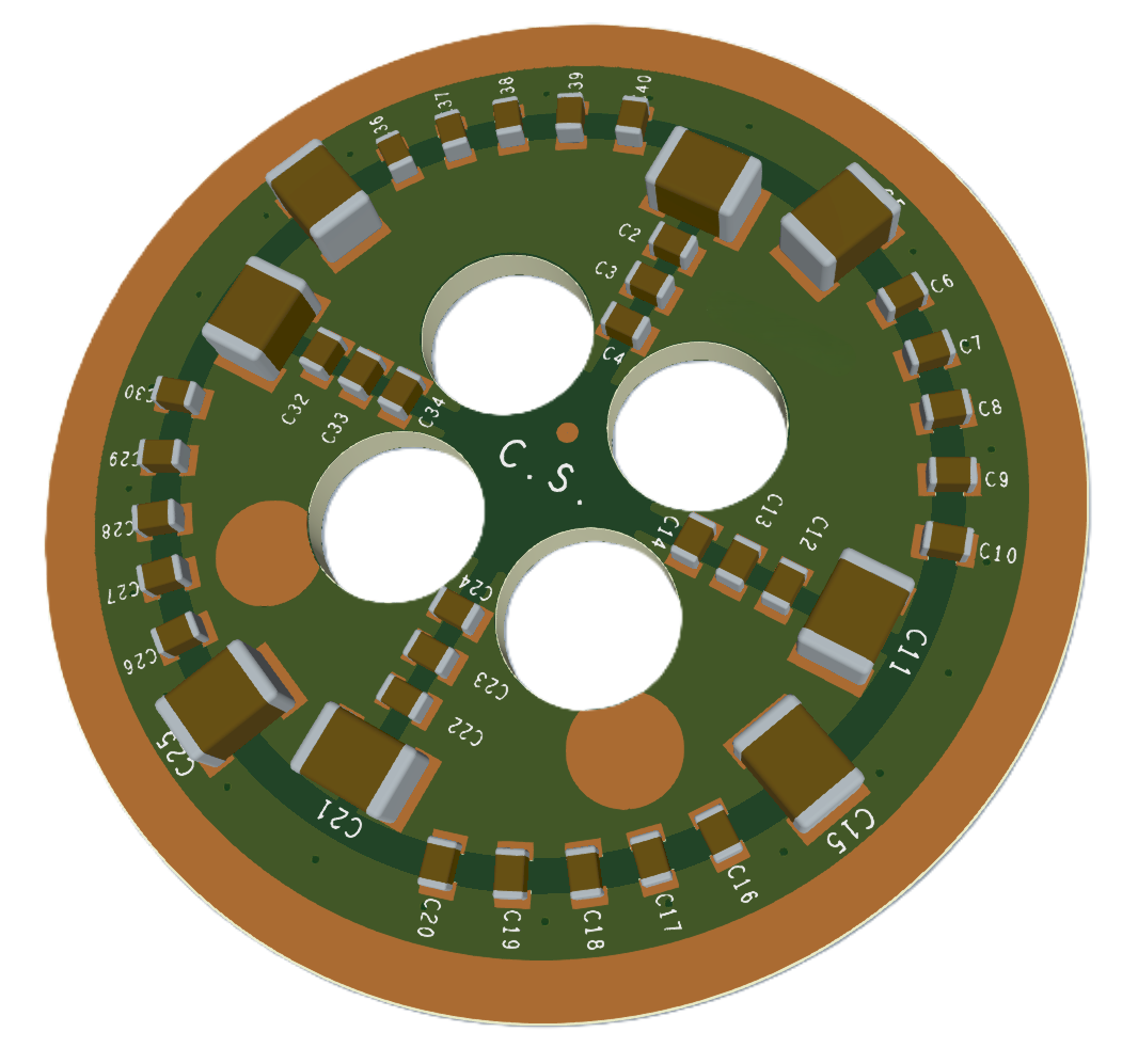
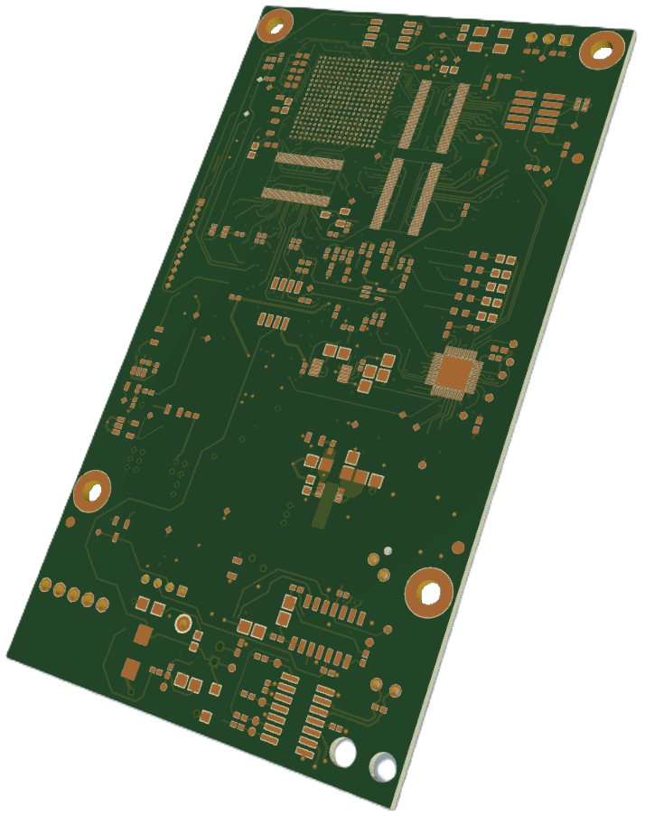
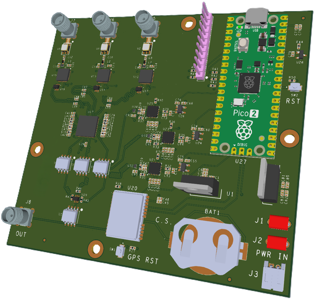
PORTFOLIO
CONTACT
Have a board that needs to work the first time?
Send over your schematics, requirements, or a rough idea. I'll reply with a scope and timeline.
Email
stanislav.rmr@gmail.com
Phone
(+972)-547806639
Response time
Within 24 hours
Based in
Israel, Karmiel